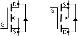
Unlike virtually every other active device, the power MOSFET is unusual in that its schematic symbol includes a parasitic device – the body diode. The body diode is intrinsic to the device’s structure. It remains despite a number of fundamental changes in power MOSFET structure and device designs including the two most common types today — planar and trench devices.

The presence of the body diode as an explicit element of the schematic symbol is an oddity. After all, we don’t pepper the MOSFET symbol with any of the three primary parasitic capacitances though they, too, affect the switch’s dynamic performance and, under suitable circuit conditions, lead to switching faults. But the body diode’s presence and behavior have become so much a part of the overall MOSFET device qualities that common circuit topologies depend on, or at least anticipate, the parametric performance of the parasitic component.
Discreet power MOSFETs also feature a parasitic bipolar transistor, but the metallization connecting the source and body regions — also an explicit feature of the schematic symbol — shorts the base-emitter junction. This prevents the bipolar device from turning on under all but the most extreme conditions. The remaining base-collector junction is in parallel with, and behaves essentially as part of, the body diode.
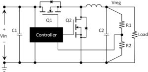
Many of the most common power MOSFET applications involve devices, in either half- or full-bridge configurations, driving inductive loads. Buck-converter topologies are a typical example. The high-side FET operates with a duty cycle D approximately equal to

When the high-side switch turns off, the inductor current has ramped to its peak for the given clock cycle. The controller will impose an amount of dead time between the high-side MOSFET turning off and the low-side device turning on to prevent shoot through (rail-to-rail conduction through the half bridge). Nonetheless, the inductor will try to maintain its current, pulling the switching node negative until the low-side MOSFET’s body diode conducts. Even after the low-side switch turns on, the body diode doesn’t turn off for a period trr, the reverse recovery time, during which charges within the PN device must recombine.
Two parts of the MOSFET’s loss model are associated with the body diode in this scenario. The first is an IL∙VD term during the diode’s conduction interval. This is significantly larger than the switch’s I 2 ∙RDS(on) loss — one motivation to minimize the switching dead time. The second is the recombination current, which adds to the inductor current flowing through the switch’s RDS(on). This results in slightly higher I 2 R losses than the circuit’s external behavior would suggest and a correspondingly higher operating temperature for the switch. Because RDS(on) exhibits a positive TCR (temperature coefficient of resistance), the device dissipation rises further, beyond that which constant-temperature calculations would predict.

Should the switching dynamics and thermal performance fall short of your circuit’s requirements, or if you’re designing for maximum energy efficiency, you can essentially eliminate the body diode’s contribution to the switch’s behavior. A Schottky diode connected in parallel to the body diode will conduct with a lower forward voltage, preventing the body PN junction from becoming forward biased. The Schottky diode is a majority-carrier device and exhibits no recombination. Be sure to use short, wide traces to connect the Schottky and the MOSFET. Even small stray inductances can reduce the Schottky diode’s effectiveness.